Kikuo Hayakawa , NOST Tokyo (Innovatie Attaché Netwerk Tokio)
Origineel gepubliceerd op de site van RVO.
De verkoop van Japanse halfgeleiders is goed voor ongeveer 10% procent van de wereldwijde verkoop. In vergelijking met 25 jaar geleden is de omvang van Japanse spelers afgenomen. Maar Japan is nog steeds een toonaangevend land op het gebied van R&D van halfgeleidertechnologie en -apparaten. Recent startte de Japanse overheid met het promoten van de ontwikkeling van toepassingen gebaseerd op halfgeleidertechnologie en -apparaten. Doel is om nieuwe markten te creëren om zo het economisch groeipotentieel te stimuleren.
Details
According to the World Semiconductor Trade Statics (WSTS), the world’s semiconductor sales totaled about 300 billion euro in 2015. The Japanese semiconductor sales account for about 10 percent of the global sales – the third largest after the US and EU. Since 1990 the number of Japanese semiconductor companies is decreasing. In 1990 there were six Japanese companies among the top 10 worldwide semiconductor sales leaders. But in 2015 only Toshiba remains on the list. (Fig.1)
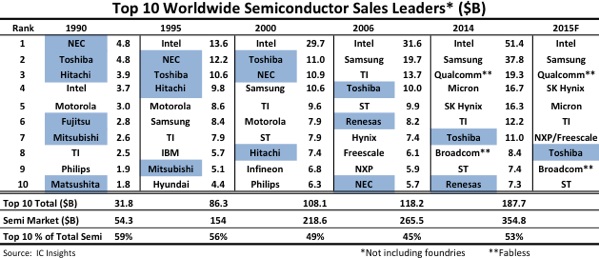
Figure 1. Top 10 Worldwide Semiconductor Sales Leaders (source: IC Insights)
Toshiba is the inventor of Flash memory used for USB memory and SSD (solid state drives) (1). The company has kept up its R&D investments at about 1.5 billion euro a year. Recently, Toshiba, Samsung, Micron and Intel and others have developed 3D NAND flash memories, drastically downsizing the memory chip. Toshiba succeeded to develop 48-layers structured NAND flash memory last year. Toshiba and SK Hynix agreed to co-develop the next generation memory. Last year Toshiba has decided to release non-core medical and other businesses. Beside that they will cut 10.000 employees by March 2016, in order to recover from their financial crisis caused by the scandal of the past illegal accounting reports. Toshiba is focusing furthermore on semiconductor business as a core business.
As other leading Japanese semiconductor companies, Sony is the world sales leader of CMOS (Complementary Metal Oxide Semiconductor) image sensors (39 percent of the market). Sony’s CMOS image sensors are used for not only digital cameras, but also smartphones including Apple’s iPhones (2). Renesas is also the world sales leader of microcomputers used for vehicles et cetera (21 percent of the market), followed by NXP/Freescale group in the market. Renesas was established in 2003 to merge with the semiconductor business of Hitachi and Mitsubishi Electric. Later the company merged with NEC Electronics. When Renesas had a financial crisis caused by the Great earthquake and tsunami Disaster in 2011, the Japanese government (through funding vehicle Innovation Network Corporation of Japan (INCJ)) saved the company through capital investments.
Recently INCJ decided to sell more than half of their stocks, because Renesas came back to profitability. Japanese DRAM (Dynamic Random Access Memory) company Elpida was established in 1999 through a merger of the DRAM business of NEC and Hitachi. Eventually, Elpida (the last Japanese DRAM maker) was integrated into Micron (US) in 2013. Sharp is one of the top 20 semiconductor sales leaders. However, the company completely lost its direction after the financial crisis due to a failure to compete in the highly price-competitive LCD (liquid crystal display) business. At this moment, Sharp is also on the way to being sold and reorganized. INCJ or Taiwan’s Ho Hai will likely be its new owner.
Semiconductor manufacturing equipment
With regards to semiconductor manufacturing equipment, Tokyo Electron is the third ranked sales leader after US Applied Materials and ASML. In 2013, Tokyo Electron and Applied Materials agreed to merge. But in 2015 they both announced to terminate the merger process, because of objections from the US Ministry of Justice. Other Japanese companies SCREEN Semiconductor Solutions, Hitachi High-Technologies, Nikon and Hitachi Kokusai Electric are listed in the top 10 worldwide semiconductor manufacturing equipment sales leaders, according to Gartner, Inc. The next generation of semiconductor manufacturing may be based on the development of Extreme Ultraviolet (EUV) lithography with a wavelength of 13.5 nano meters. A Japanese light source module company Gigaphoton, an important supplier to ASML, has developed 60W EUV, using funding from the Japanese governmental R&D funding organization NEDO (New Energy and Industrial Technology Development Organization) (3). The company is developing to reach a high power 250W EUV source needed to produce semiconductor chips. The Gigaphoton’s EUV source is integrated with the advanced CO2 amplifiers developed by Mitsubishi Electric. Gigaphoton and Mitsubishi Electric collaborate in a joint project: Innovative Center for Coherent Photon Technology (ICCPT) led by University of Tokyo. ICCPT aims to develop new production systems using light sources such as EUV. ICCPT is one of the projects under the Japanese governmental long-term program Center of Innovation (COI) Program, funded between 2013 and 2021 (4).
MEMS market
The Japanese government will start the new five-year Science and Technology Basic Plan from April 2016. The plan aims to promote R&D in technologies necessary to create a smart society. IoT (Internet of Things) and sensor technologies are identified as key areas to help its realization. Actually, MEMS (Micro Electro Mechanical Systems) sensors, based on silicon-based devices, are widely used for smart vehicles, smartphones, tablets, smart glasses and other wearable devices. MEMS is one of key elements for IoT. According to Yole Développement (Yole), the MEMS market was 12.3 billion euro in 2014. And Yole reported that it will exceed 22.2 billion euro in 2020. The top 30 MEMS players in the world include several Japanese companies; Denso, Panasonic, Alps, Omron, EPSON, Canon, Murata and Sony (4). (Fig. 2)
Opportunities for the Netherlands
Holst Centre, the Eindhoven-based open innovation centre driven by TNO and Belgian Imec, is leading with its ultra-low power wireless technologies. Holst Centre has done joint-research agreements with Japanese companies including Omron, Fujitsu and Rohm. Regarding sensor technologies, Japan has a special demand on road infrastructure. The road infrastructure monitoring system project has started aiming to monitor conditions of old tunnels and bridges using MEMS sensors since 2014. The five years project was triggered by a fatal accident of ceilings falling down in an old tunnel of Japanese highways in 2012. A MEMS association Micromachine Center of Japan (MMC), universities and companies are involved in the project financed by the Japanese R&D funding organization NEDO. Durable MEMS sensors and sensing systems are targeted to develop. MMC is also leading other projects of sensor technologies regarding high-efficiency micro energy harvesting devices, innovative recognition systems for autonomous driving and next-generation cow monitoring systems.
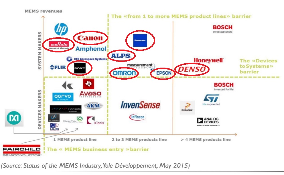
Figure 2. Top 30 MEMS players’ positioning: devices vs. systems vs. number of MEMS product lines (source: Yole Development)
New semiconductor devices
A new innovative type of flash memory B4 ( Back Bias assisted Band to Band tunneling ) flash memory has been developed by Genusion, a Japanese startup based in Kawasaki (6). The B4-Flash memory is a NOR-typed memory, enabling 200 times faster than the conventional NAND type at reading data. Genusion’s B4-Flash memory received the innovation award from NOKIA in 2008. The company has been developing B4-Flash memory technologies funded by NEDO.
As new power semiconductors, SiC (silicon carbide) and GaN (gallium nitride) based semiconductors are expected to highly improve energy efficiency. The R&D project of SiC and GaN power electronics has been funded by the Japanese governmental organization JST (Japan Science Technology Agency), and conducted under the Super Cluster Program in Kyoto and Aichi (7). This five-year program has started in 2013 with a total budget of about 40 million euro. In Japan, the recent developments on SiC power devices are especially highlighted. In Japan it is foreseen that the whole replacement by SiC power devices saves 30 Tera Wh (equal to three or four nuclear power plants). SiC power devices were invented by Prof. Matsunami, Kyoto University, Japan in the 1970’s. Japan’s Rohm started the first mass production of SiC MOSFET (Metal-Oxide-Semiconductor Field-Effect Transistor) in 2012, in cooperation with Kyoto University and Tokyo Electron. Rohm, German Infineon and US Wolfspeed are leading with SiC developments. The Kyoto-based Super Cluster Program is led by Advanced Science Technology & Management Research Institute of Kyoto (ASTEM) in cooperation with universities and companies in the Kyoto area. The Program promotes new systems using SiC power devices for various applications including electricity transmissions, invertors, and motors. Meanwhile, Toyota, Denso and Toyota Central R&D Labs have developed high efficiency SiC power devices for hybrid vehicles in 2014. They conducted a successful test on public roads in May 2015. The Toyota group aims to downsize the power control unit of vehicles using SiC power devices by 20 percent, and improve the energy efficiency by 10 percent. Toyota will start installing SiC power devices in its cars around 2020 (8-9).
Currency:
1 US dollar is 1.11 euro (22 February 2016)
1 euro is 125 yen (22 February 2016)
Sources:
- Toshiba, the Inventor of Flash Memory
- Nikkei Gyokai Chizu (Nikkei Industry Map) 2016 (in Japanese)
- NEDO: EUV Light Source with 60WGigaphoton
- COI Program – Innovative Center for Coherent Photon Technology (ICCPT)
- Yole Development: Growing in maturity, the MEMS industry is getting its 2nd wind
- Genusion – B4 flash memory
- JST: Super Cluster Program – power electroncis
- Toyota develops chips for hybrid cars to boost fuel efficiency
- Toyota proves an efficency test with SiC power deveice (in Japanese)


