Kikuo Hayakawa, NOST Tokyo
Origineel gepubliceerd op de site van Agentschap NL.
Samenvatting
Japan ziet micro-elektromechanische systemen (MEMS) als een belangrijke bijdrage in de strijd tegen milieuproblematiek en vergrijzing. Door nieuwe publiek-private projecten investeert Japan in een nieuwe markt voor MEMS-technologieën op het gebied van milieu/energie, gezondheidszorg en veiligheid/beveiliging.
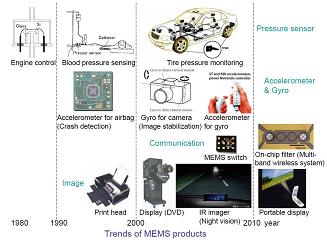
Microelectromechanical systems (MEMS) are tiny mechanical devices that are built onto semiconductor chips and are made up of components between one to a hundred micrometers in size (0.001 to 0.1 mm). MEMS usually consists of a central unit that processes data, a microprocessor and several components that interact with the outside, such as microsensors. In research labs since the 1980s MEMS devices began to materialize as commercial products in the mid-1990s. They are used to make pressure, temperature, chemical and vibration sensors, light reflectors and switches as well as accelerometers for airbags, vehicle control, pacemakers and games. The technology is also used to make inkjet print heads, microactuators for read/write heads and all-optical switches that reflect light beams to the appropriate output port. Cars, inkjet printers, mobile phones, digital cameras and games are currently major consumer applications for MEMS devices (Fig. 1). The MEMS world market has grown by 15% in the past four years. In general, the US leads the R&D in many fields of MEMS technologies at universities and industry. Europe is advanced on production technologies for MEMS and fundamental research at universities. Japan is advanced on user applications with MEMS devices , such as games, digital cameras and robots, and on cooperation with governmental R&D projects among universities, research institutes and industries.
Figure 1. Trends of MEMS products (source: Tohoku University)
Developments for Japanese clients
According to the major French marketing and consulting company Yole Développement, in 2009 the total MEMS world market was US$7 billion – a 25% increase of 2005. The top 30 MEMS developers and manufacturers account for 72% of the world market . The top MEMS company is US Texas Instruments (TI). TI is advanced on the development of digital micromirror devices, which are known through the company’s core technology of digital light processing (DLP). The Japanese companies Mitsubishi Electric and PLUS apply it for respectively projection TV and video projectors. The fourth ranked French ST Microelectronics is advanced on 3-axis acceleration sensors (accelerometer for gyro), which is applied for a motion-activated user interface to the worldwide popular Wii. Wii has been firstly developed by the Japanese world-largest game console company Nintendo. The top thirty includes six major Japanese companies such as Canon, Seiko Epson and Panasonic. Canon and Seiko Epson are major inkjet printer manufacturers which use their own inkjet print heads. Panasonic is involved in the development of pressure and gyroscope sensor devices for among others cars and car navigation systems. According to Yole Développement the most notable development of this year is the gyroscope market, which is led by the rapidly growing American company InvenSense. InvenSense has introduced the world’s first integrated MEMS gyroscope, with a price of less than US$3. The low-cost manufacturing is realized by Taiwanese foundry TSMC. Japanese camera companies such as Sony and Olympus use the gyro chip from InvenSense for their digital cameras with the function of image stabilization.
Governmental projects
In order to promote R&D on MEMS technologies in Japan, the Japanese government has launched MEMS projects since 1991. Below three major R&D governmental projects are introduced, which aim to contribute to the bottom-up of Japanese MEMS developments.
– BEANS project (2008-2012)
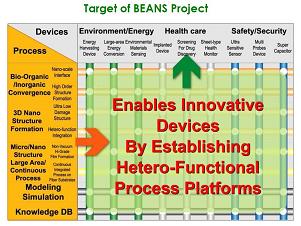
Bio Electro-mechanical Autonomous Nano System (BEANS) is a Japanese governmental MEMS project. Projectleader Prof. Hiroyuki Fujita from the University of Tokyo believes MEMS to be very important for Japan. Fujita: “It is said in Japan that semiconductor chip is rice for the industry, as rice provides energy for the human body. Beans contain proteins for bio functions, such as eyes for sensing and muscle for actuation. MEMS are hoped to become beans for the industry.” BEANS is the third generation of MEMS projects under the Japanese ministry METI, with a budget of four million euros for five years. The second generation was called the ‘Fine-MEMS’ project and focused on MEMS manufacturing process development. The BEANS project aims to develop the hetero-functional integrated device technology, which includes four research subjects: bio-organic/inorganic materials convergence process, novel fabrication technology for 3D nano-structures, large area continuous process of micro/nano structure and the construction of a knowledge database. The final target products are in three different sectors: environment/energy conservation, healthcare and safety/security (Fig. 2). The BEANS project is joined by sixteen companies (such as Olympus, Panasonic and Terumo), several universities, the National Institute of Advanced Industrial Science and Technology (AIST) and four research institutions like the Micromachine Center in Japan. The objective is to realize a US$22 billion market on Japanese MEMS-applications in 2015, most of this based on the BEANS project.
Figure 2. Target of BEANS project (source: BEANS project)
- Projects for Microsystem Integration led by Tohoku University and AIST
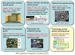
The MicroSystem Integration Center of Tohoku University is one of the most successful MEMS research organizations in Japan. It has two governmental MEMS-related R&D projects. One is the Micro System Integration Initiative and runs from 2007 to 2016. The project is funded by MEXT, the Japanese Education ministry, with a total budget of three million euros. The project aims to develop next generation wireless systems, sensor networks, functional sensors, optical microsystems, biomedical microsystems and fabrication test equipment. Fourteen Japanese companies, like Ricoh and Toppan, participate in the project (Fig. 3).
Another MEMS project has just been approved by the Japanese Cabinet Office and is part of the ‘World-leading innovative R&D division program’. This project runs until 2013 and has a budget of 2.5 million euros. The project leaders are Prof. Esashi of Tohoku University and Dr. Ryutaro Maeda, director of the N-MEMS research center at AIST. Objective of the project is to develop initial stage prototyping for hetero integration, hands-on access to fabrication facilities and massive parallel Electron Beam exposure systems. Prof. Esashi has set up a MEMS park consortium to improve MEMS knowledge and skills by means of training programs and technical seminars since 2004. Currently a hundred Japanese companies are members of the consortium.
Figure 3. Micro System Integration Initiative 2010 (source: Tohoku University)
- GMEMS (Green MEMS)-project (2009-2014)
GMES was separately launched to develop green fabrication technologies to reduce electricity consumption in clean rooms. MEMS technologies are expected to apply a new micro energy management system in a chip, which manages energy reduction at home, in data centers and in offices. Dr. Ryutaro Maeda of AIST is also in charge of this project. The project is joined by sixteen Japanese companies, such as Omron and Mitsubishi Electric, and has a budget of six million euros for six years.
International collaborations
Prof. Esashi of Tohoku University has been collaborating with the Fraunhofer Research Institute in Germany on Electronic Nano-Systems and MEMS materials development, with IMEC in Belgium and the Italian Politecnico di Torino on bio-MEMS. Prof. Esashi would like to collaborate with more foreign research institutes and universities. Dr. Maeda, AIST, is open to exchange information with foreign university researchers. The possibilities for collaboration with foreign companies are limited due to the industry partnership of Japanese governmental projects such as BEANS.
Sources
- Micromachine Center – http://www.mmc.or.jp/
– “Tsukuba Innovation Arena (TIA) on Nanotechnology”, Intl. Workshop, Feb.2010
– BEANS project: http://www.beanspj.org/
– Prof. Isao Shimoyama, University of Tokyo: http://www.leopard.t.u-tokyo.ac.jp/
– Tohoku University: http://www.mems.mech.tohoku.ac.jp/
– National Institute of Advanced Industrial Science and Technology (AIST): http://www.aist.go.jp/
– MEMS park consortium: http://www.memspc.jp/
– Micromachine/MEMS 2010 Tokyo: http://www.micromachine.jp/


