Kikuo Hayakawa, NOST Tokyo
Originally published on the site of NL Agency
Summary
Japan foresees that the future office will not be comparable to today’s office with regard to information quantity and speed (1). The future office will be more productive and efficient, based on more advanced computers with electric devices and composed materials, allowing larger capacities and higher speeds. At the same time, computer components should be more energy efficient to contribute to a low-carbon society.
The Japanese government has stimulated this development through focused research and development. There are seven major research projects going on through the New Energy and Industrial Technology Development Organization (NEDO). The projects focus on research into high-performance devices, low-power devices and infrastructure technologies. Within these projects universities cooperate with companies. One of the already completed projects through NEDO, the die-bonding film, has been commercialized for embedded components such as smartphones. Just like this project, NEDO hopes that the ongoing projects will contribute to the promotion of the future office.
Details
Currently, demand for information quantity and speed rapidly increases in Japan due to the large amount of smart phones and the popularity of cloud computing. The seven NEDO-projects focus on:
(1) The development of infrastructure for normally-off computing technology;
(2) Extremely low-power circuits and systems (Green IT Project);
(3) Low power electronics project for a low carbon emission society;
(4) Development of functionality innovative three-dimensional integrated circuit technology (Dream Chip);
(5) The development of next-generation semiconductor micro-fabrication and evaluation infrastructure technologies;
(6) The development of nanobit technology for ultra-high density magnetic recording (Green IT Project);
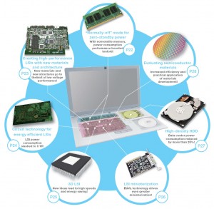
(7) The consortium for advanced semiconductor materials and related technologies (fig. 1).
Fig. 1. Future office: various approaches to improving performance and power saving (Source: NEDO)
- The development of infrastructure for normally-off computing technology
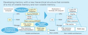
This project focuses on development of high speed and large capacity non-volatile memory which leads to zero power consumption in standby mode (fig. 2). Conventional computers need power even in a standby mode, because their hierarchical structure needs to use a volatile memory such as SRAM. Under a new structure using both volatile and non-volatile memories, computers such as smart phones with zero standby power consumption come within reach. The project, which runs from 2011 until 2015, is led by Prof. Hiroshi Nakamura of the University of Tokyo. Toshiba, Rohm, NEC group and Renesas all participate. The budget will be 45 million Euros in total.
Fig. 2. Developing memory with a new hierarchical structure allowing normally-off properties (source: NEDO)
- Extremely low-power circuits and systems (Green IT Project)
This project aims to achieve ninety percent reduction in power consumption of Large-scale Integrated Circuits (LSI) with an extremely low voltage below 0.5 Volts. To realize this, it focuses on the development of logic, memory, analogue and power source devices.
Other approaches in the project are the development of technology for optimizing integration of devices into LSI chips and wireless / inter chip communication circuits and multi-core technology using software to control power consumption by using a standard Complementary Metal Oxide Semiconductor (CMOS) process. In this project for the period 2009-2012 ten companies and universities participate, such as the Semiconductor Technology Academic Research Center, System LSI Co. and University of Tokyo. The budget is 32 million Euros in total.
- Low power electronics project for a Low carbon emission society
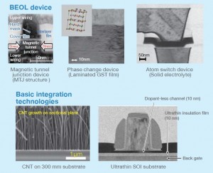
This project aims to challenge the limits of power reduction in LSI by using new devices based on new materials such as carbon nanotubes and graphene. It focuses on the development of non-volatile memories that store data by resistance values fabricated in a Back-End Of Line (BEOL) process as well as basic integration technologies leading to reduction of power consumption in LSI.
BEOL is a wiring process within LSI processes. NEDO regards BEOL devices as devices fabricated in a BEOL process with the use of new materials. The targeted devices are: magnetic tunnel junction devices to store information on the direction magnetization, phase change devices to store information on the basis of differences in the crystal structure of phase change materials and atom switching devices that realize the electric connection and disconnection by formation and annihilation of metal bridges between electrodes (fig 3). The development of basic integration technologies targets to create low resistance wirings and plugs, by using graphene for wirings and carbon nanotubes for plugs. It also targets to create variation-free low power CMOS devices using a 10-nm ultrathin insulation film (fig. 3). The devices under development should meet the specifications of required applications with low voltage and reduced power dissipation. The project (2010-2014) is joined by the Low Power Electronics Association and Project. The budget is 110 million Euros in total.
Fig. 3. BEOL devices and basic integration technologies (source: NEDO)
- The development of functionality innovative three-dimensional integrated circuit technology (Dream Chip)
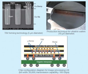
The current approach of two-dimensional miniaturization of wire length in semiconductors will meet its limits in about ten years, according to Moore’s law. This project focuses on the three-dimensional layering technology to respond to market demand for higher speed and lower energy consumption. One of the necessary elements for this future technology is to produce through-silicon via (TSV) for shorter wires and less resistance. This project succeeded to produce a five micro meters diameter TSV. The wafer in the wiring layer achieved a ten micro meters ultrathin structure (fig. 4). The project (2008-2012) is led by Prof. Kazuya Masu of Tokyo Institute of Technology and joined by the Association of Super-Advanced Electronics Technologies. The budget is 83 million Euros.
Fig. 4. TSV forming technology and ultrathin wafers (source: NEDO)
- The development of next-generation semiconductor micro-fabrication and evaluation infrastructure technologies
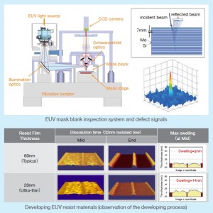
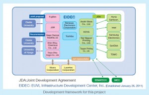
This project aims to develop the new mask and resist technologies which will form the new extreme ultraviolet EUV lithography systems. EUVL is the next-generation of lithography using a 13.5 nanometers extreme ultraviolet beam, instead of the conventional 193 nanometers wavelength beam. EUVL is one of basic technologies for LSI miniaturization. The new mask should have defect-free multiple layers of reflective and absorbing coatings. The new mask should be designed for patterns of less than twenty nanometers width, which should be newly developed. This project focuses on the development of EUV mask defect inspection technology to guarantee the quality of the mask materials. It also focuses on the development of EUV resist materials with ten to sixteen nanometers level resolution performance (fig. 5). This project (2011-2015) is led by Dr. Hisamitsu Watanabe of the EUVL Infrastructure Development Center (EIDEC)(2) and joined by 21 companies and universities such as Fuji film and Osaka University (fig. 6). For NEDO this is the first project joined by foreign companies in order to evaluate the research and development subjects. The budget is 83 million Euros in total.
Fig. 5. Development of a EUV mask defect inspection system and resist materials (source: NEDO)
Fig. 6. Development framework for the EUVL project (source: NEDO)
- The development of Nanobit Technology for Ultra-high Density Magnetic Recording (Green IT Project)
This project aims to develop ultra-high density nanobit magnetic media technology, which will contribute to the reduction of power consumption of storage systems such as a hard disks. Generally, hard disks account for more than twenty percent of the total power consumption in a data centre. This project targets to create hard disks with a memory density of five terabits per square inch, which is ten times the conventional memory density. It is expected to achieve a more than twenty percent power consumption in data centres as a result of the smaller size and amount of hard disks. It focuses on the development of ultra density nanobit magnetic media, ultra high performance magnetic heads, ultra high nano-addressing technology and hard disk drive systems. This project (2008-2012) is led by Dr. Yoshihiro Shiroishi of Hitachi and joined by Toshiba. The budget is 40 million Euros in total.
- The Consortium for Advanced Aemiconductor Materials and related Technologies
The target of this project is to develop an evaluation technology for advanced materials for three hundred millimetre wafer. It focused on the development of special wiring test-element-groups (TEGs) with junction devices and the related material evaluation technologies. The project, which ran from 2009 to 2011 was led by the Consortium for Advanced Semiconductor Materials and related Technologies (CASMAT) (3) and joined by the Japanese leading semiconductor materials manufacturers such as JSR and Toray. The project finished on March 2012. The summary report will be published in October. The budget was 1.3 million Euros in total.
Commercialized die-bonding film technology
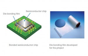
One of NEDO’s completed projects regarding new materials was the die-bonding film produced by Hitachi Chemical. It is by now successfully launched on the semiconductor market. The nano-scale phase separation mechanisms have been found by Prof. Takashi Inoue of Yamagata University and the entailed integrating bonding technologies have been developed by Hitachi Chemical, funded through NEDO’s Nanostructure Polymer Project (2001-2007)(fig. 7). Hitachi developed technology for the nano-level control of the phase decomposition structure of the acrylic polymer and epoxy resin (4). Currently Hitachi Chemical’s die-bonding film accounts for more than fifty percent of this market. It is becoming a de facto standard in the technology of multilayer mounting of semiconductors. It is an essential technology for embedded components in smartphones and tablets. Hitachi Chemical received the Japan’s Prime Minister Award with this die-bonding film in September 2011. Like this project, NEDO hopes that the ongoing projects will contribute to the stimulation of the office of the future.
Fig. 7. Die-bonding film technology (source: NEDO and Hitachi Chemical)
Currency
One Euro is 101 yen (as of September 24, 2012)
Source
(1) NEDO – Future Office (page 11-15)
(2) EUVL Infrastructure Development Center, Inc
(3) CASMAT

