Kikuo Hayakawa, NOST Tokyo
Originally published on the site of NL Agency.
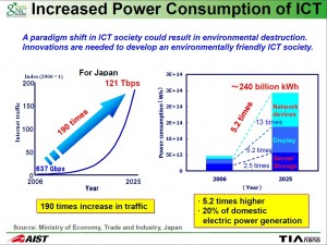
The Japanese power consumption of ICT equipment is predicted to be 240 billion kWh in 2025, which is 5.2 times that in 2006. Green nanoelectronics are expected to contribute to the reduction of the power consumption of electric devices such as LSIs, one of the major power consuming elements of ICT equipment. In Japan, the Green Nanoelectronics Center (GNC) of the National Institute of Advanced Industrial Science and Technology (AIST) plays the major role in green nanoelectronics research. It is funded by the Japanese government and joined by Japanese companies (Renesas, ULVAC, Fujitsu, Toshiba, Hitachi), seven universities and two research institutes. GNC also implements the research programs gathered at an open innovation cluster called ‘Tsukuba Innovation Arena’ (TIA-nano). AIST is recently in contact with IMEC in Belgium and Holst Center in the Netherlands.
Details
On March 14, 2012, the International Symposium on ‘Development of Core Technologies for Green Nanoelectronics’ was held in Tokyo. The symposium was organized by the Green Nanoelectronics Center (GNC) of the National Institute of Advanced Industrial Science and Technology (AIST). Green nanoelectronics are defined as ultralow-power electronics, value-added by nanotechnology and/or nanomaterials. The Japanese power consumption of ICT equipment is predicted to be 240 billion kWh in 2025, which is 5.2 times that of 2006, due to the 190 times increase in traffic (figure 1). It will account for twenty percent of the total electric power generation in Japan. Green nanoelectronics are expected to contribute to the reduction of the power consumption of electric devices such as LSIs, which are one of major power consuming elements of ICT equipment. The GNC’s project has an objective to develop core technologies to reduce the power consumption of electric devices by a factor of 1/100 by the end of the project in March 2014.
Figure 1. Increased power consumption of ICT (source: Ministry of Economy, Trade and Industry)
Green Nanoelectronics Center (GNC) in AIST
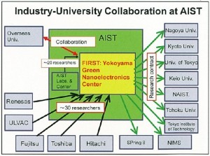
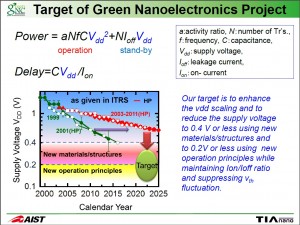
AIST is one of Japanese major research institutes. AIST is involved in more applied sciences than pure science, like the Dutch TNO. GNC was established in AIST in April 2010, and will be operated until March 2014. The research at GNC is funded by the Japan Society for the Promotion of Science (JSPS) through the Funding Program for World-Leading Innovative R&D on Science and Technology (FIRST). FIRST aims to encourage the leading-edge research and development that will strengthen Japan’s international competitiveness and contribute to the society and people’s welfare by sharing the results (1). The total budget of FIRST is 952 million euro. The GNC’s green nanoelectronics project, one of thirty projects of FIRST, has a budget of 47 million euro. Dr. Naoki Yokoyama, who came from Fujitsu, is the head of this project, joined by Japanese companies (Renesas, ULVAC, Fujitsu, Toshiba, Hitachi), seven universities, and two research institutes (figure 2). This project has three subthemes to develop core technologies for reducing the power consumption of LSIs by a factor of 1/10, and eventually by a factor of 1/100: 1) Low voltage operation CMOS; 2) Development and application of nanocarbon materials; 3) Material research for backend devices (2). The target of this project is to reduce the supply voltage to 0.4 V or less by using new materials/structures on CMOS (such as InAs/Ge), and also to 0.2 V or less by using new operation principles on CMOS (such as grapheme) (figure 3).
Figure 2. Industry-University Collaboration at AIST Green Nanoelectronics Center (source: AIST)
Figure 3. Target of Green Nanoelectronics Project (source: AIST)
Nanoelectronics R&D in TIA nano
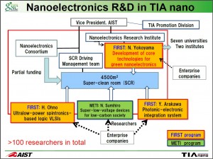
GNC also implements the research programs gathered at an open innovation cluster called ‘Tsukuba Innovation Arena’ (TIA-nano) and works with the universities and research laboratories throughout the country. GNC accelerates the research by taking advantage of the large-scale research infrastructure which was built at TIA-nano (1). TIA-nano is a nanotechnology cluster cooperated by the University of Tsukuba, AIST, and the National Institute for Materials Science (NIMS). With regards to nanoelectronics there are three different projects of FIRST (including GNC) and two projects funded by METI (Ministry of Economy, Trade and Industry) in TIA-nano. In total more than a hundred nanoelectronics researchers are working in TIA-nano. AIST is recently in contact with IMEC in Belgium and Holst Center in the Netherlands.
Figure 4. Nanoelectronics R&D in TIA-nano (source: AIST)
Currency:
1 euro = 105 yen (as of April 17, 2012)
Sources:
1) Collaborative Research Team Green Nanoelectronics Center, AIST – http://www.yokoyama-gnc.jp/
2) International Symposium on “Development of Core Technologies for Green Nanoelectronics”, March 14, 2012, Tokyo, organized by AIST
3) Tsukuba Innovation Arena – http://tia-nano.jp/en/index.html
| nano in NIMS |


